The photovoltaic industry is one of the largest volume markets for reflectance-based film thickness gauges, for a plain reason: cell production is counted in gigawatts, every cell carries films that need measuring, and those films happen to grow squarely inside the comfort zone of reflectance-based measurement. This article covers two representative scenarios.
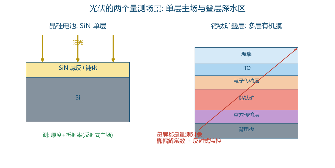
The first is the silicon nitride antireflection (AR) coating on crystalline-silicon cells. SiN plays a double role on the cell: optically it is an antireflection coating, pushing down the reflection losses of the silicon surface (bare silicon reflects over 30%; after coating, single digits); process-wise it is a passivation layer, with chemical passivation reducing surface recombination. Both roles are thickness-sensitive: the antireflection effect is governed by the optical thickness n·d (the quarter-wavelength condition), while the passivation effect correlates with the deposition process window. What the line must control is two quantities — thickness and refractive index — plus full-panel and batch-to-batch uniformity. The reflectance-based film thickness gauge scores nearly full marks on fit for this scenario: a single transparent layer, clear fringes, and millisecond-to-second speed to match the line's takt. Across the industry, large numbers of lines use reflectance-based gauges for 100% inspection or high-ratio sampling.
The second is perovskite and tandem (stacked) cells. The film stacks here are far more complex: the perovskite absorber is sandwiched between the electron transport layer and the hole transport layer, and with the transparent electrodes and substrate the stack starts at five or six layers. Most of the materials are organic or hybrid, dispersion models must be built from scratch, samples are soft (no touching), areas are small, and process drift between batches is large. Joint reflectance-based and ellipsometry measurement is the realistic scheme: ellipsometry solves the optical constants and ultrathin layers, reflectance-based measurement does fast process monitoring. This scenario demands far more from software than from hardware — the prior-knowledge logic of "Single-Layer, Double-Layer, and Multilayer Films" applies.
Photovoltaics adds two industry-specific requirements on the instrument. First, size and takt: full-panel mapping must keep up with the line, and inline form factors (line-scan style, on the order of several thousand points per second) are increasingly common — Acuitik's NS-100 high-speed line-scan film thickness gauge is designed for exactly such scenarios, officially rated at millisecond-level single-point measurement and several thousand points per second in line scan. Second, environmental tolerance: shop-floor dust and temperature/humidity fluctuations must be absorbed in the instrument's design, and the convenience of calibration (see "Calibration Standards, Calibration, and Traceability") directly determines uptime.
One closing lesson: most selection mistakes by photovoltaic customers come from "comparing only single-point accuracy and never full-panel throughput". The line's real problem is uniformity monitoring of thousands of cells per hour; however high the single-point accuracy, a mapping step half a beat slow is the bottleneck. Do the takt accounting first, then look at accuracy specifications.
About Acuitik
Acuitik specializes in optical precision measurement technology. Its core products are reflectance-based film thickness gauges, ellipsometers, and OEM film thickness sensors featuring "non-contact, non-destructive, sub-nanometer accuracy":
- Industrial film thickness measurement NS series: NS-20 manual, NS-30 automated Mapping, NS-Micro microscopic, NS-Touch curved-surface, NS-HR thick-film, NS-100 high-speed line-scan
- Research-grade measurement ES series: ES-Tenso ellipsometer, ES-Primo multi-wavelength ellipsometer (for ultrathin films and complex multilayers), plus the NS-Vista dual-channel and NS-Flex portable multimodal units
- OEM film thickness sensors: multi-point nanoscale film thickness, NS-HR thick-film, and NS-Micro microscopic sensor modules, supporting Modbus / OPC UA for integration with PLC and MES, with an SDK provided
The instruments are metrologically certified by the National Institute of Metrology of China and the Shanghai Institute of Measurement and Testing Technology, and Acuitik participated in drafting the group standard T/CIET 2298-2026 "Calibration Specification for Thin-Film Interference Film Thickness Measurement Systems". For more selection guides and application notes, please visit the Acuitik official website.