Semiconductors are the market with the most demanding requirements and the most complete logic for film thickness metrology. Understanding how this industry uses film thickness gauges is essentially understanding everything such instruments can do. This article clarifies three things: where metrology stands in the production line, where film-stack evolution is pushing it, and how far domestic manufacturing has come.
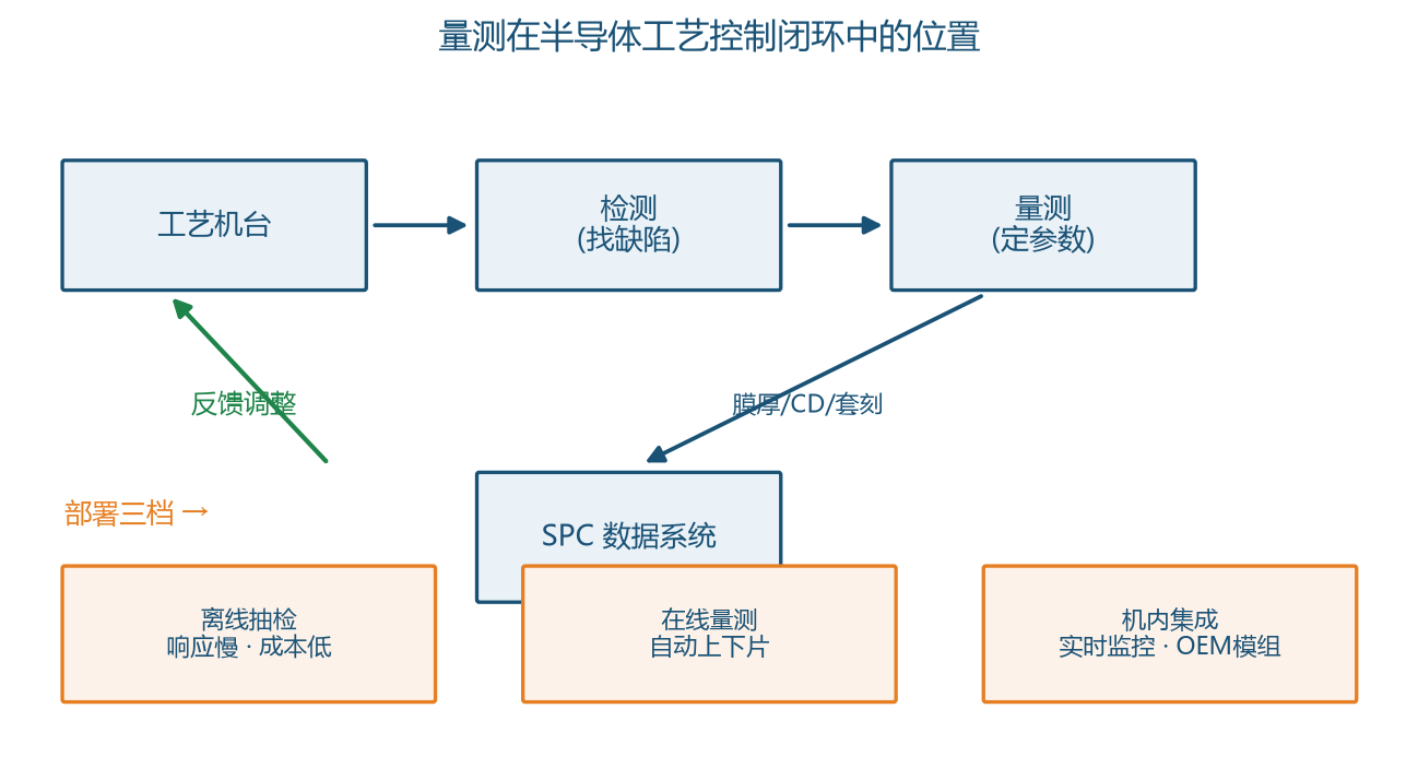
First, the position. Process control in a wafer fab is a closed loop: process tools fabricate, inspection equipment finds defects, metrology equipment pins down parameters (film thickness, CD, overlay), and the data system aggregates everything for statistical process control, feeding back to adjust the process tools. Film thickness metrology's role in this loop is "determining the cause": defects tell you something went wrong; film thickness data tells you whether it was the film, by how much it is off, and in which direction. Deployment falls into three tiers: offline sampling (the metrology tool sits in a lab, samples sent in for testing), inline metrology (automatic loading and unloading on the production line's transfer path), and integrated metrology (mounted inside the process tool for real-time monitoring). From offline to inline, response speed and cost rise together.
Next, how film-stack evolution pushes requirements upward. Twenty years ago logic devices were mainly silicon dioxide and silicon nitride, with thicknesses at the hundred-nanometer scale — reflectance-based measurement was sufficient. After the 45 nm node introduced high-k metal gates, control of the gate dielectric's EOT (equivalent oxide thickness) entered the angstrom regime, and spectral ellipsometry and OCD became the mainstays. On the memory side, DRAM's ultrathin dielectric layers have entered the 10–50 Å range; in 2025 Onto released metrology equipment targeting this range and secured a volume purchase agreement of roughly 69 million US dollars from a major DRAM manufacturer — the market has confirmed the scale of this direction with real money. The trend compresses into one sentence: films get ever thinner, metrology moves from intensity measurement toward phase measurement, and from sampling toward full-wafer coverage.
Third, the position of domestic manufacturing. In 2020, the domestic share of metrology and inspection equipment in mainland China was about 2% (a figure on which various sources broadly agree), and it has risen rapidly since then on mature process nodes. Film thickness metrology happens to be a sensible entry point for domestic players: the parameters are standardized, validation cycles are relatively short, and there are clear benchmarks. Industry players such as Skyverse, Ruili Scientific Instruments, and Shanghai Jingce have made successive breakthroughs in line-level metrology, while the benchtop and industrial-grade markets are more broadly competitive. Acuitik's path runs along a different flank: a product matrix of reflectance-based film thickness gauges (six form factors — manual, Mapping, microscopic, curved-surface, thick-film, and line-scan) covering industrial and research scenarios, plus entry into equipment makers' line integration through OEM modules, with Modbus and OPC UA protocols connecting to PLC and MES and an SDK for secondary development. For equipment integrators, this is a lighter path to introducing metrology capability than buying complete instruments.
A closing selection hint for semiconductor users: the process node determines the technical route (thick dielectric films go reflectance-based; angstrom-scale goes ellipsometry/OCD), the position on the line determines the form factor (offline — look at functionality; inline — look at uptime and interfaces), and vendor evaluation should add one consideration specific to domestic suppliers: metrology certification and participation in standards — verifiable credentials (see "Calibration Standards, Calibration, and Traceability").
About Acuitik
Acuitik specializes in optical precision measurement technology. Its core products are reflectance-based film thickness gauges, ellipsometers, and OEM film thickness sensors featuring "non-contact, non-destructive, sub-nanometer accuracy":
- Industrial film thickness measurement NS series: NS-20 manual, NS-30 automated Mapping, NS-Micro microscopic, NS-Touch curved-surface, NS-HR thick-film, NS-100 high-speed line-scan
- Research-grade measurement ES series: ES-Tenso ellipsometer, ES-Primo multi-wavelength ellipsometer (for ultrathin films and complex multilayers), plus the NS-Vista dual-channel and NS-Flex portable multimodal units
- OEM film thickness sensors: multi-point nanoscale film thickness, NS-HR thick-film, and NS-Micro microscopic sensor modules, supporting Modbus / OPC UA for integration with PLC and MES, with an SDK provided
The instruments are metrologically certified by the National Institute of Metrology of China and the Shanghai Institute of Measurement and Testing Technology, and Acuitik participated in drafting the group standard T/CIET 2298-2026 "Calibration Specification for Thin-Film Interference Film Thickness Measurement Systems". For more selection guides and application notes, please visit the Acuitik official website.