Eighty percent of data problems with reflectance-based film thickness gauges come from the sample, not the instrument. This article breaks down the three most common types of "difficult samples" one by one — symptom, mechanism, remedy — and can be used directly as a troubleshooting manual.
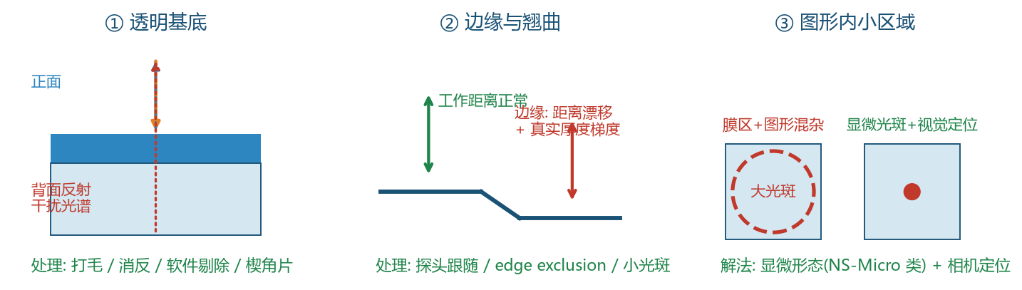
Type one: transparent substrates. When films are coated on glass, sapphire, or quartz substrates, the front-side reflectance spectrum superimposes with the reflection from the substrate's backside; the fitting treats the backside signal as part of the film and the thickness comes out systematically biased. Remedies, from lowest to highest cost: the software method (modern fitting software can add a backside-reflection model or reject long-path components — try this first); the physical method (roughen the backside by sandblasting or grinding to destroy its specular reflection — the most thorough, but it damages the sample); the antireflection method (coat the backside with anti-reflection wax or matching liquid and wipe it off after measuring). One more often overlooked: wedged substrates (glass with a slight wedge angle) steer the backside-reflected light out of the detector's field of view and are naturally immune to this problem — you can deliberately choose wedged glass when procuring transparent substrates.
Type two: edges and warpage. Within a few millimeters of a wafer's or cover plate's edge, film thickness genuinely has a physical gradient (the edge effect of coating processes); add edge warpage that shifts the working distance and slopes that push the incidence angle off its calibrated value, and the data is often "all bad at the edge." Treat the two separately: real edge thickness variation must be measured with a proper edge strategy (a small spot plus precise edge positioning, or accepting the edge-exclusion convention — most industry specifications simply exclude the outer 1–5 mm); warpage, meanwhile, calls for probe following (autofocus or a contour-following stage) to keep the working distance within the depth of field.
Type three: small patterned areas. Patterned wafers, cover plates with openings, multi-zone samples — the measurable area may be only millimeters or even a few hundred micrometers across. A conventional millimeter-scale spot would illuminate film and non-film regions at once, mixing the signals. The solution is a microscopic optical path: a small spot (micrometer-scale) plus coaxial vision positioning — first locate the target region in the camera, then place the spot. The configuration costs more than a standard model, but for patterned products there is essentially no alternative.
Beyond the three types, several high-frequency minor pitfalls are worth listing as well: ambient stray light (at stations hit by direct sunlight, stray light enters the spectrum and raises the baseline — a light shield on the probe solves it); film-surface contamination (fingerprints and particles inside the spot are scattering sources — blow off with air or clean before measuring, the most cost-effective procedure there is); the sample resting on its backside (set it on spacer particles so the backside hangs free — for transparent substrates this also mitigates backside reflection); vibration of the motion stage (reading before the stage has settled during mapping shows up as regular sawtooth anomalies in the data — wait for the settle signal or add a delay to eliminate it).
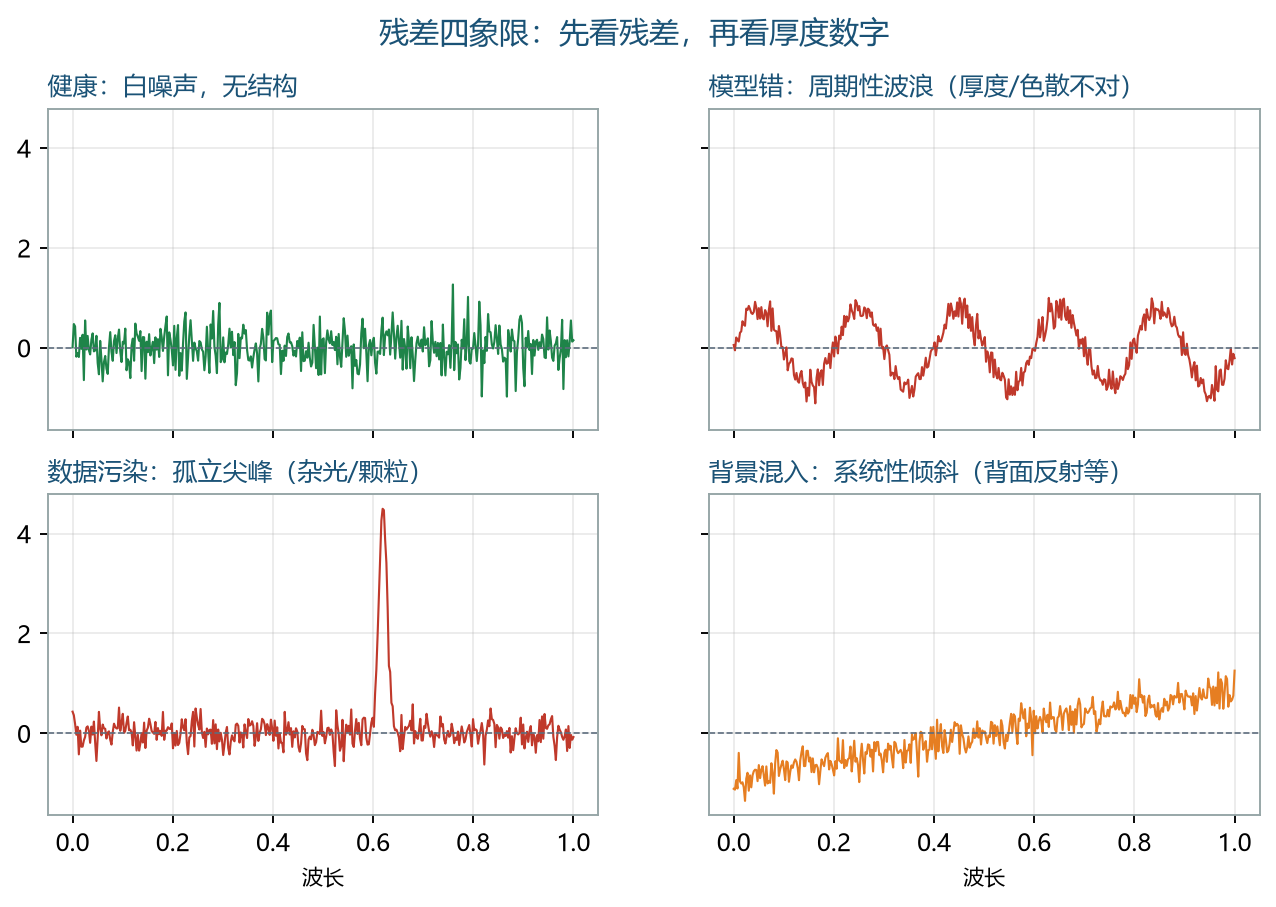
Fix a standard troubleshooting order: first check how well the fitted curve matches the measured spectrum (the problem is in the model), then re-measure at a different position (the problem is sample uniformity), and finally verify with a calibration standard (the problem is the instrument). After these three steps, the vast majority of "the data looks wrong" cases can be localized. For deeper puzzles, ship the sample to the vendor's application laboratory for comparative measurement — major vendors such as Acuitik all offer this service, and it is far faster than grinding through it alone.
About Acuitik
Acuitik specializes in optical precision measurement technology. Its core products are reflectance-based film thickness gauges, ellipsometers, and OEM film thickness sensors featuring "non-contact, non-destructive, sub-nanometer accuracy":
- Industrial film thickness measurement NS series: NS-20 manual, NS-30 automated Mapping, NS-Micro microscopic, NS-Touch curved-surface, NS-HR thick-film, NS-100 high-speed line-scan
- Research-grade measurement ES series: ES-Tenso ellipsometer, ES-Primo multi-wavelength ellipsometer (for ultrathin films and complex multilayers), plus the NS-Vista dual-channel and NS-Flex portable multimodal units
- OEM film thickness sensors: multi-point nanoscale film thickness, NS-HR thick-film, and NS-Micro microscopic sensor modules, supporting Modbus / OPC UA for integration with PLC and MES, with an SDK provided
The instruments are metrologically certified by the National Institute of Metrology of China and the Shanghai Institute of Measurement and Testing Technology, and Acuitik participated in drafting the group standard T/CIET 2298-2026 "Calibration Specification for Thin-Film Interference Film Thickness Measurement Systems". For more selection guides and application notes, please visit the Acuitik official website.