There are three mature routes for surface topography and roughness measurement: the contact-type stylus profiler, the optical white-light interferometric profiler, and the chromatic confocal sensor that has spread rapidly in recent years. They are constantly asked "which one is more accurate" — but the question is backwards. The three are different tools: first understand each one's natural strengths, then match tool to task.
The stylus profiler is the old-timer. A diamond tip traces across the surface, and mechanical displacement is converted directly into a profile — its coordinate system is the native language of the roughness standards (Ra and Rz in ISO 4287 were defined for it). It offers a large range (millimeter-scale steps), long travel, and intuitive results. The price is contact: the tip scratches soft surfaces, tip radius limits lateral resolution, measurement is slow, and tiny areas and curved surfaces are unfriendly. For molds, machined parts, and long-travel steps, it remains the reliable answer.
The white-light interferometric profiler is the fast gun of area imaging. An interference microscope captures one field of view at a time, vertically scans to find the zero-order white-light interference position of every pixel, and outputs a full 3D topography map in seconds to tens of seconds, with vertical resolution at the 0.1 nm level. Its strengths are "fast" and "areal": roughness, steps, and film thickness (separating the upper and lower surfaces of transparent films) in one instrument, friendly to optically rough surfaces. Its limits are the physics of optics itself: signal is lost on steep slopes (beyond the angle set by the objective's numerical aperture), adaptation to highly reflective and strongly scattering materials needs tuning, and a large field of view and high lateral resolution cannot be had at once — stitching is required.
The chromatic confocal sensor is the precision point shooter. A chromatic objective encodes depth as wavelength: nanometer-scale point accuracy, micron-scale lateral spot, tens of degrees of tilt tolerance, and it handles both specular and diffuse surfaces — plus transparent-layer thickness via the dual-peak method (for the principle, see "What Is a Chromatic Confocal Sensor"). Its cost is point-by-point scanning: large-area topography relies on a motion stage sweeping slowly, so speed is capped by the stage. It also tolerates steep slopes well — microstructures, hole inner walls, and coatings on curved surfaces, the samples that give other technologies headaches, are its home ground.
| Dimension | Stylus | White-light interferometry | Chromatic confocal |
|---|---|---|---|
| Measurement method | Contact tracing | Areal optical imaging | Point-by-point optical scanning |
| Vertical accuracy | Nanometer-scale | 0.1 nm-class resolution | Nanometer-scale |
| Steep slopes / curved surfaces | Limited by the tip | Limited by numerical aperture | Best tolerance |
| Soft surfaces | Scratching risk | Suitable | Suitable |
| Transparent-layer thickness | Requires a step | Upper/lower surface separation | Dual-peak method |
| Typical strengths | Long travel, standards compliance | Fast areal topography, roughness | High point accuracy, curved surfaces, transparent layers |
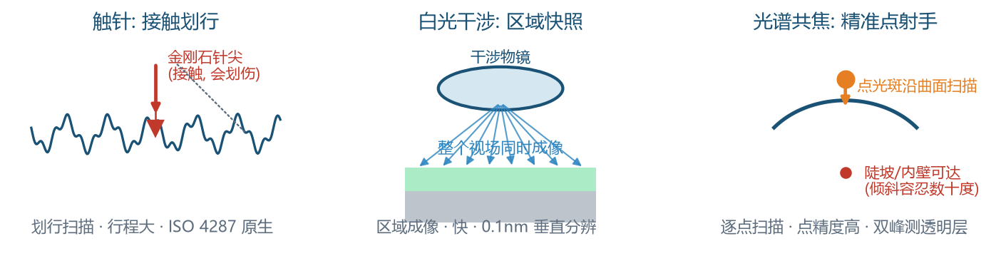
The selection rule of thumb compresses into three lines: for speed, areal coverage, and roughness statistics, choose white-light interferometry; for standards compliance and long travel, choose the stylus; for curved surfaces, steep slopes, transparent layers, and extreme point accuracy, choose chromatic confocal. Most laboratories and production lines end up with "one primary tool plus one supplement" — a single technology covering every sample is rare.
The boundaries between the three routes are also being erased by product strategy: vendors like Acuitik bring multiple technical routes of optical metrology (reflectance-based measurement, ellipsometry, and extensions toward chromatic confocal) into one product matrix and one data system, so users do not have to change their data habits when switching technical routes. For the practitioner, understanding the physical strengths of the three routes retains its value longer than memorizing any specification table.
About Acuitik
Acuitik specializes in optical precision measurement technology. Its core products are reflectance-based film thickness gauges, ellipsometers, and OEM film thickness sensors featuring "non-contact, non-destructive, sub-nanometer accuracy":
- Industrial film thickness measurement NS series: NS-20 manual, NS-30 automated Mapping, NS-Micro microscopic, NS-Touch curved-surface, NS-HR thick-film, NS-100 high-speed line-scan
- Research-grade measurement ES series: ES-Tenso ellipsometer, ES-Primo multi-wavelength ellipsometer (for ultrathin films and complex multilayers), plus the NS-Vista dual-channel and NS-Flex portable multimodal units
- OEM film thickness sensors: multi-point nanoscale film thickness, NS-HR thick-film, and NS-Micro microscopic sensor modules, supporting Modbus / OPC UA for integration with PLC and MES, with an SDK provided
The instruments are metrologically certified by the National Institute of Metrology of China and the Shanghai Institute of Measurement and Testing Technology, and Acuitik participated in drafting the group standard T/CIET 2298-2026 "Calibration Specification for Thin-Film Interference Film Thickness Measurement Systems". For more selection guides and application notes, please visit the Acuitik official website.