Using NS-20 Max film thickness gauge to achieve atomic-level precision thin film measurement, supporting nano-scale thin film characterization in cutting-edge research fields such as new superconducting materials and microfluidic chips.
Optical reflection film thickness measurement technology principle
Optical reflection film thickness gauge uses high-stability broadband light vertically incident on the sample surface. Optical interference occurs between each film layer, and the reflected light undergoes spectral analysis and regression algorithms to calculate the thickness of each film layer. It is suitable for measuring thickness, reflectance, refractive index and other parameters of transparent or semi-transparent films ranging from nano-scale to micro-scale.
NS-20 Max applications in cutting-edge research fields
Perfluoropolyether (PFPE) coating can modify the surface of biological gene detection chips through chemical bonding or physical adsorption, adjusting the surface hydrophilicity/hydrophobicity to better meet various requirements during detection, such as uniform sample distribution, reducing non-specific adsorption, thus improving detection accuracy and sensitivity.
PFPE coating thickness has important correlation with friction coefficient, liquid loading capacity, and wear resistance, making thickness measurement crucial.
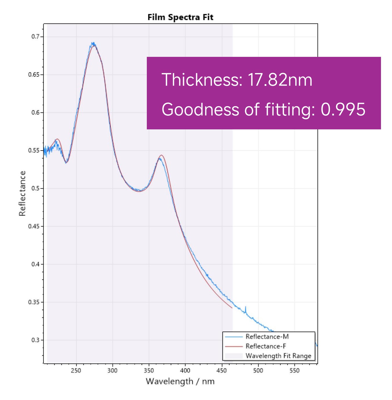
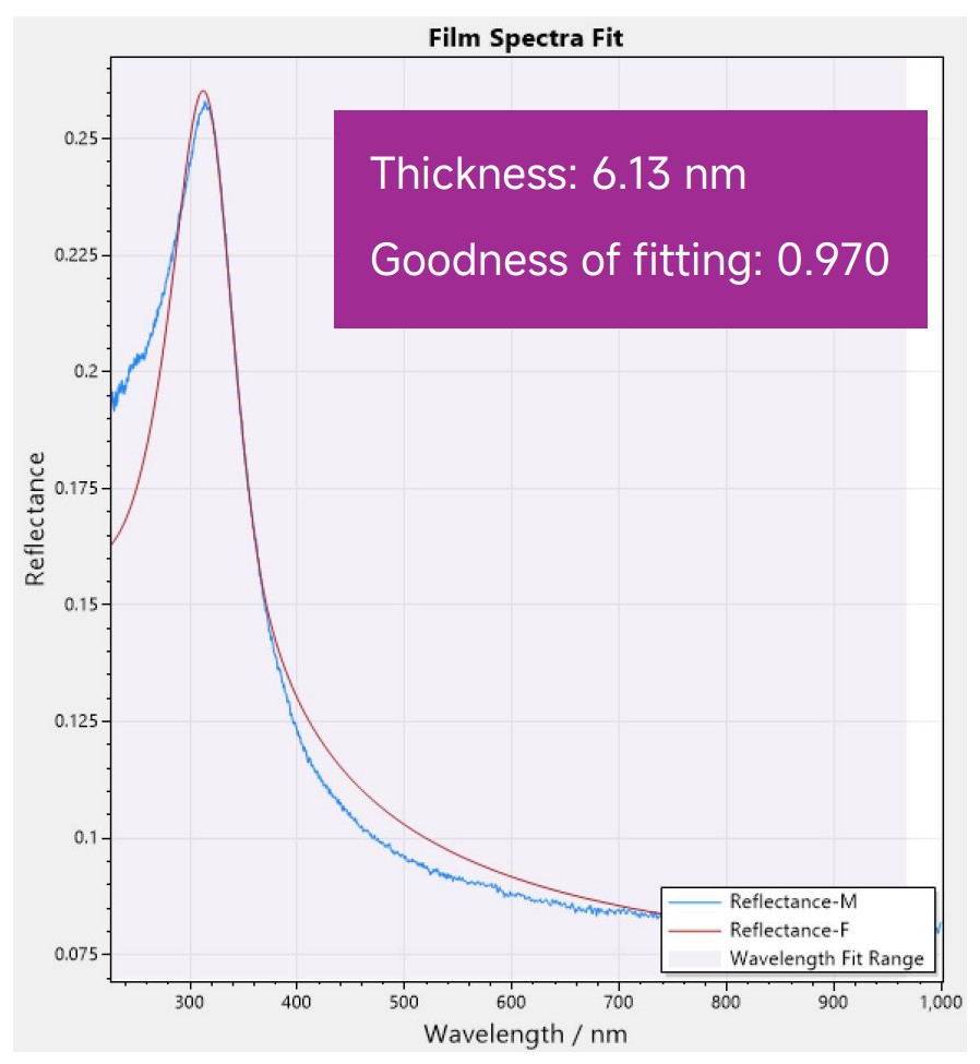
Acuitik NS-20 Max film thickness gauge measurement results for 10~20 nm PFPE coating thickness are as follows:
In 2025, a Chinese scientist team successfully achieved atomic-level layer-by-layer controlled synthesis of high-quality (La, Pr)₃Ni₂O₇ epitaxial films on NiO (nickel oxide) substrates, observing both zero resistance and complete diamagnetism, two hallmark characteristics of superconductors. This provides new ideas and methods for nickel-based superconductor research and applications.
Using Molecular Beam Epitaxy (MBE) technology, in a high vacuum environment, lanthanum oxide components are used as beam sources, deposited layer-by-layer on NiO substrates. Atomic-level precision thin film fabrication is achieved by precisely controlling deposition rate and growth temperature parameters. Film thickness control here requires very high accuracy and real-time monitoring.
Acuitik's reflection film thickness gauge can be integrated in vacuum for real-time measurement of 0.1 nanometer thickness changes, providing a reliable measurement foundation for scientific exploration of high-temperature superconducting properties.
Unique advantages of NS-20 Max in nano-scale thin film measurement
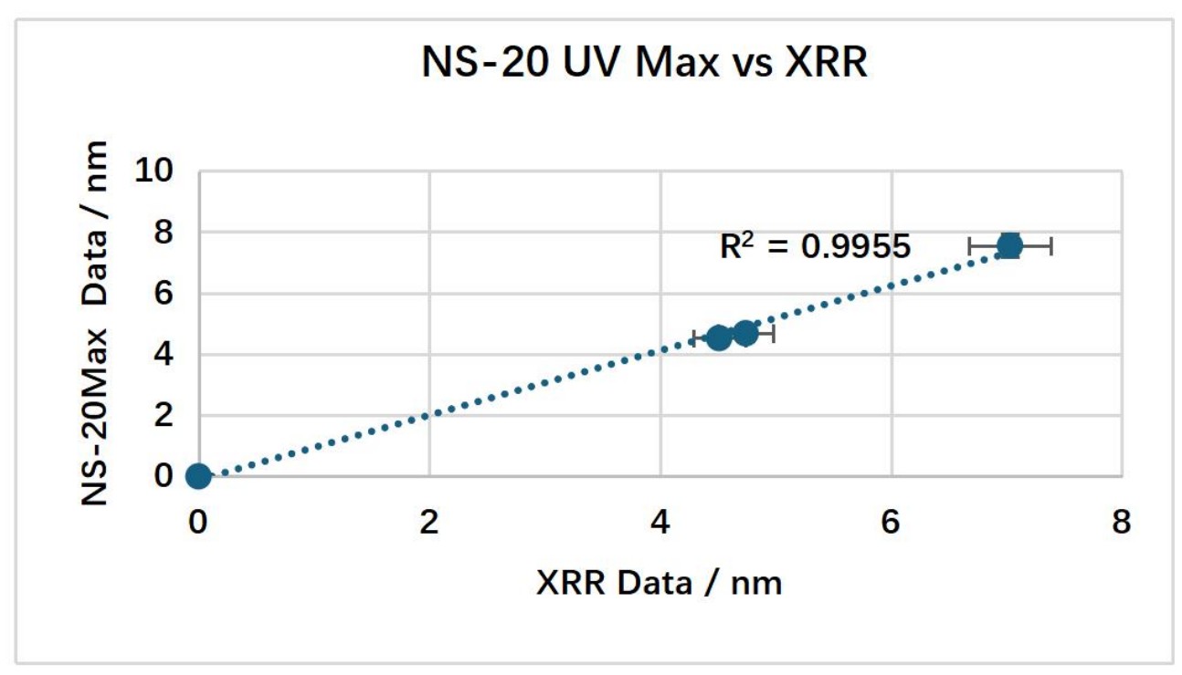
Comparing measurement results of LaO thin films of different thicknesses with XRR (X-ray Reflectivity) instruments. Notably, the NiO substrate is semi-transparent, and its refractive index is close to that of LaO, which is extremely difficult for conventional optical thickness measurement.
It can be seen that for ultra-thin films of just a few nanometers, Acuitik's reflection film thickness gauge has a measurement deviation within 1 nanometer. This is due to Acuitik's high-stability algorithm and optical design.
Compared with XRR technology, there is a gap in measurement precision for films a few nanometers thick with optical film thickness gauges. However, Acuitik optical film thickness gauges can be easily integrated in vacuum in-situ measurement environments or vacuum-connected chambers, enabling simultaneous growth and measurement, further improving experimental efficiency for scientists exploring new materials.
Contact our technical team for high-precision thin film measurement solutions for your cutting-edge research projects