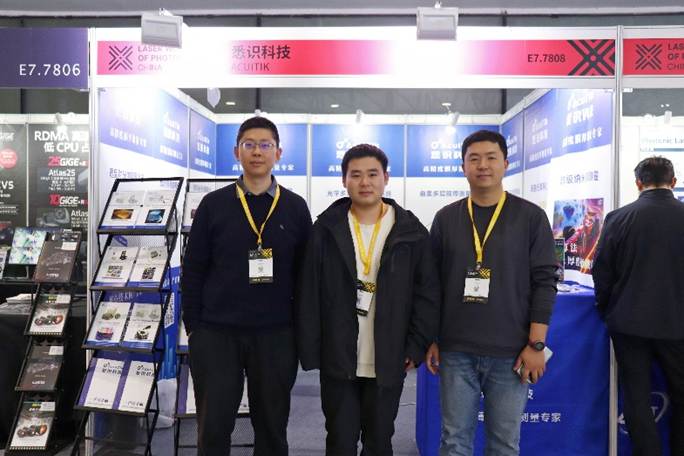
On March 18, 2026, Laser World of Photonics China opened grandly at Shanghai New International Expo Center. As an important event in Asia's laser, optics, and optoelectronics industry, this exhibition brought together many well-known enterprises and technical experts from around the world. Acuitik showcased its NS-20 Non-Destructive Coating Thickness Gauge for Advanced Packaging at the exhibition, focusing on semiconductor advanced packaging inspection pain points and demonstrating innovative breakthroughs in domestic optical precision measurement equipment.
Core Technical Advantages
- • Non-contact measurement: Complete measurement without touching samples to avoid damage
- • Micro spot: Achieve micron-level precise positioning detection
- • Multi-layer film analysis: Support complex multi-layer film structure analysis
- • High precision, non-destructive, intelligent film thickness measurement
Acuitik's booth (E7.7808) attracted many industry professionals and customers to visit and exchange. Through live demonstrations and technical exchanges, Acuitik showcased its deep accumulation and innovative strength in the field of optical precision measurement to the industry.